IBE離子束刻蝕系統北京特博代理美國IBE離子束刻蝕系統--功能強大----科研用戶。
| 主要用途 |
| 1. Ion Beam Etching to fabricate micro-nanometer features in any material (metals, insulators, organics, composites, multilayers). 2. Ion Beam Surface Modification to create nanostructures, textures and smoothness. 3. Physical Vapor Deposition to build thin films and stacks by evaporation, sputtering and reactive growth. 4. Ion Beam Sputter Deposition confronts the need for upper tier thin film results, when achieving the highest quality properties and precision control is justified. |
| 優勢 |
| Multifunctional Process Tool combines etching and deposition in one vacuum process chamber. |
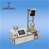
| 系統構成 刻蝕圖例 |
|
  |
| 應用領域 |
| 1. Semiconductor 2. Nanotechnology 3. Photonics 4. Spintronics |
| 適應的刻蝕材料 |
| 1. Noble Metals ; 2. Insulators 3. Diamond Films 4. Optical Wave Guides 5. Superconducting Materials 6. Magnetic Materials |
| 工藝能力 |
| 1. Ion Beam Etching (IBE) 2. Reactive Ion Beam Etching (RIBE) |
|

|

|

|

|

|
*您想獲取產品的資料:
個人信息:


